

Applications
Discover what you can reach with most advanced hybrid pixelated detectors for electron microscopy.
(4D) STEM in SEM/TEM
AdvaScope detectors are built for modern 4D STEM workflows, capturing complete diffraction data at every probe position with exceptional speed, precision, and sensitivity. Our hybrid pixel detectors record individual electron events without noise and unlimited dynamic range, enabling accurate reconstruction of strain, magnetic fields, phase information, and atomic-scale structure. One of the key strengths of this detector in 4D STEM applications is its data-driven readout approach. Rather than capturing a complete image at every probe position, the detector streams individual detection events directly from the sensor. This enables extremely short dwell times down to hundreds of nanoseconds thusremoving the conventional image acquisition bottleneck and significantly accelerating data collection. A complete map of 1536 x 1024 points can be acquired in up to 80 seconds.
What this means for users:
- Reliable, quantitative 4D STEM datasets
- Faster acquisition with minimal sample damage
- Superior contrast and precision in challenging experiments
With AdvaScope, 4D STEM becomes not just powerful, but practical and routine. (YouTube link)


EBSD (Electron Backscatter Diffraction)
AdvaScope brings step-change improvements to EBSD performance. Thanks to direct electron detection our detectors deliver high-speed, low-noise acquisition with crisp diffraction pattern definition even on difficult materials thus enabling robust indexing and higher mapping throughput.
What this means for users:
- Cleaner Kikuchi patterns for improved indexing success
- Higher-speed acquisition without sacrificing quality
- Enhanced performance on low-signal or challenging samples
For quality assurance, materials characterization, and manufacturing control, AdvaScope enables EBSD users to see more, faster.
EELS (Electron Energy Loss Spectroscopy)
EELS demands precision and AdvaScope delivers it. Our detectors provide precise timing and single-electron sensitivity, improving energy resolution and signal quality even for weak edges and light elements.
What this means for users:
- Better signal-to-noise performance
- Clearer detection of subtle chemical shifts
- Faster data collection for beam-sensitive samples
From battery interfaces to semiconductor devices, AdvaScope enables deeper chemical understanding at the nanoscale.
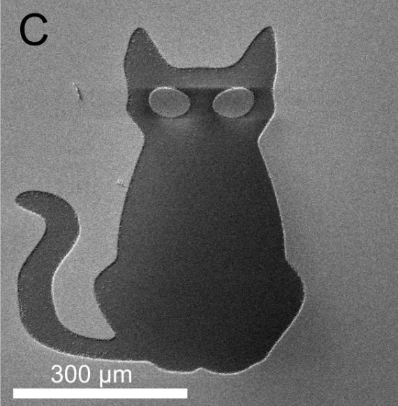
This photo was obtained by TU Wien and that we use it with their curtesy.
Micro Electron Diffraction (µED)
µED relies on clean, sharp diffraction patterns from crystals that are too small for traditional X-ray techniques. AdvaScope detectors excel in this domain, delivering exceptional sensitivity and dynamic range to capture both strong and extremely weak reflections with clarity.
What this means for users:
- High signal quality for accurate structure solutions
- Excellent low-dose and low-energy performance for fragile crystals
- Fast readout enabling efficient workflows
From pharmaceuticals to advanced materials, AdvaScope detectors ensure µED produces results you can trust.
Unlimited Dynamic Range
Hybrid pixel detectors* provide a combination of data per contact with electrons and display outstanding dynamic range and sensitivity. The technology is able to show diffraction spots on silicone in one picture with kikuchi lines. It also shows amazing results on nickel using backscattering.
*also known as photon counting detectors (PCDs) or photon counting pixel detectors (PCPDs)

Bespoke Software Solutions
We provide a software development kit with each detector, which allows customers to implement the data they have obtained into their own imaging program. With our technology, you get precise results in real-time!